What is strain analysis?
Strain in semiconductor devices is a vast and important subject. Instinctively, one could be tempted to think of strain as a sort of mechanical failure – think cracks when the strain is too high – but strain can also be used to influence the electronic properties of semi-conductors, and is used as so in strain engineering [1, 2, 3, 4, 5].
Raman spectroscopy is an ideal technique for measuring strain, as it is sensitive to even very small changes in the crystalline lattice. It also offers high spatial resolution for the precise analysis of electronics elements, down to a few hundred nano-meters using classic Raman and a few nanometers in TERS (tip-enhanced Raman spectroscopy).
Generally speaking, strain analysis can be quite complex. Strain is the result in materials of applied stress (which can be deformation, lattice mismatch or doping, for example). Depending on the direction of the stress with respect to the crystalline structure of the material, strain can propagate differently. A very comprehensive explanation of this subject is given in an excellent article by Ingrid De Wolf [6].
Example of analysis of a silicon chip
In this example, we analyzed strain measurements made on a silicon chip using Raman spectroscopy. The metal part induces the mechanical strain in the silicon in the vicinity of the interface.
To simplify this analysis, we will suppose here that strain is uniaxial [6]. The relation between stress σ and peak shift Δω is linear and described as [6,7]:
σ[MPa]= -500 × ∆ω[cm-1]
The peak shift to higher wavenumbers means the sample is under compressive stress and the peak shift to lower wavenumbers indicates tensile stress.
Peak fitting
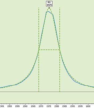
To analyze peak shift due to strain, peak fitting is used. Peak fitting uses mathematical functions, mainly Gaussian or Lorentzian in spectroscopy, to describe in a consistent way a real – measured – peak with parameters such as peak position, peak width or peak area. In the picture below, the blue line corresponds to a measured spectrum and the green line corresponds to the fitting function.
Data pre-processing
Data visualization and pre-processing are two preliminary steps necessary for correct analysis. In MountainsSpectral® the Hyperspectral image view allows versatile visualization of spectral data with a large choice of display options in order to obtain all the information necessary to determine pre-processing steps.
In this case, the following pre-processing steps were chosen to prepare the data for analysis:
- Reducing the spectral region of analysis around of the peak of interest (Extract slices operator)
- Bringing all the spectra to the baseline = 0 (Correct the baseline operator)
- Removing spectra taken on the metal part, which doesn’t contain any Raman information (Clean up or Extract area operator)
- Removing the effect of the tilted surface (Normalize operator)
Obviously, these steps should always be adapted to the data and to the analysis which will follow.
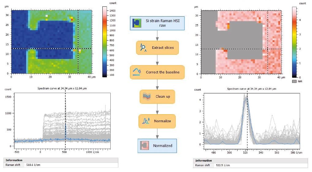
Above. Pre-processing steps applied to spectral data
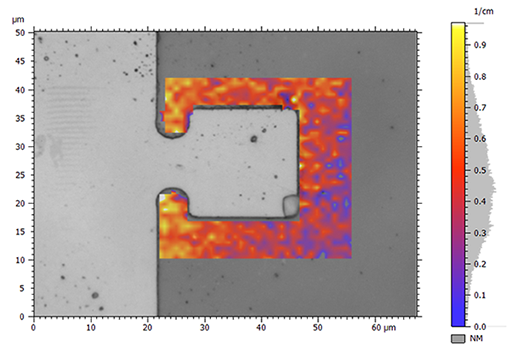
Above. Optical microscopy image of the silicon chip studied overlaid with peak shift parameter map
Data analysis
The Peak fitting study and Parameter map operator were used to perform the peak fitting and to visualize results.
We will focus here on the image directly above which represents the distribution of the peak shift of the peak of interest from its ideal non-strained position which is 520.7 cm-1. We can see that, close to the metal pin, the silicon is strained because the peak shift is about 1 cm-1. As the peak position shifts to higher values, it indicates compressive strain. At a certain distance from the metallic pin, the shift peak values become closer to 0, which demonstrates relaxation (no strain) of the silicon.
References
[1] I. De Wolf, “Raman Spectroscopy: about chips and stress”, SpectroscopyEurope, 2003, www.spectroscopyeurope.com/system/files/pdf/Raman_15_2.pdf
[2] en.wikipedia.org/wiki/Strain_engineering
[3] Lue Tao et al 2020 “Recent advances in mechanical strain engineering of low-dimensional semiconductors and their applications in high-performance quantum emitters”, Semicond. Sci. Technol. 35 103002, iopscience.iop.org/article/10.1088/1361-6641/ab8e0b#sstab8e0bs3
[4] Minamisawa, R. et al., “Top-down fabricated silicon nanowires under tensile elastic strain up to 4.5%”, Nat Commun 3, 1096 (2012) www.nature.com/articles/ncomms2102
[5] Yongke Sun, Scott E. Thompson, Toshikazu Nishida, “Strain Effect in Semiconductors”, Springer, 2010
[6] I. De Wolf, “Micro-Raman spectroscopy to study local mechanical stress in silicon integrated circuits, Semicond. Sci. Technol. 11 (1996) 139–154, iopscience.iop.org/article/10.1088/0268-1242/11/2/001
[7] G. Sarau et al., “From Micro– to Macro–Raman Spectroscopy: Solar Silicon for a Case Study” in “Advanced Aspects of Spectroscopy”, InTech, 2012 DOI: 10.5772/2757, www.intechopen.com/chapters/38553
Instruments & software used
Raman spectroscopy & MountainsSpectral®
Author
Renata Lewandowska, product manager for spectral applications at Digital Surf